Tait 8100 VFO Display Modification
These are the display modifications required to the display, so, once
done it will fit on to the main board and case when it is time for
assembly.
This page is soley for the VFO kit for the Tait 8100.
You can find the main project page here
Tait 8100 VFO Interface
.
Please note, I take no credit for this modification and please read my
Disclaimer
and you understand it before
continuing.
Photo 1. Display.
This is the display before any modifications are done.
Read through these instructions FIRST and then do the modifications so
you are clear on what to do.
Photo 2.
Photo 2 shows a close up of the front side corner that needs to be cut
off. Be very careful here not to cut to close to the display itself. The
cutters will clip off the corner in one snip.
Using a medium size pair of side cutters, cut the corner as shown in the
photo 2. and photo 3 shows the rear side cut off.
Tip.
You can mark the board first with a vivid marker, to double check you
have the right corner, before you cut.
Photo 3.
Shows the rear of the display with the modified corner cut off the PCB
board.
Photo 4. Links J1 and J4 ONLY are Required.
In order for the display to work correctly you will need to check which
links are joined. You will see in the close up in photo 4, these links
marked J1, J2, J3, J4.
We only need J1 and J4 to be made as seen in the photo.
Some displays already come with these links done so if your display
shows solder over the half moon ONLY on J1 and J4 then they are in the
right place, and you do not need to do anything.
If solder is on any of the other links, J2 or J3 then you will need to
remove these links.
Removal of the Links.
You will notice these links are made by soldering 2 half moon shapes
together.
The best way to remove these links is by using solder wick.
Place the solder wick over the link you are to remove and apply the
soldering iron and wiping off the excess solder.
Make sure the link is completly removed.
The end result, you will have only, J1 and J4 links joined.
If you need help with this, see Rob ZL1RJS or your local club.
Testing the Display.
With the club building this kit, some of us have found that some
displays have been assembled with the backlight diodes reversed.
To do a simple test now to make sure your backlight is working, put 5v
on pin 15 of the display, and fit a 100 ohm resistor on pin 16 to 0V.
(Pin 15,16 are located towards the center of the PCB.)
See the photo below to show the pin numbers.
If the backlight lights up blue, then you are good to go.
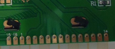 Display Pin Numbers
No Backlight.
Only do this next step if you have no blue backlight.
links, 1 and 4 are the correct links, BUT because some have found that
the backlight diodes are incorrectly assembled you will need to try
changing the links over so J2 and J3 should be shorted J1 and J4 open.
Once the backlight is lighting up blue, then continue and proceed to the
next step.
Photo 5. Bending the Tabs Over
Photo 5 shows a close up of the tabs that need to be bent over.
Be carful on doing this. There are 8 tabs in total that need to be done.
Using a small pair of pliers, turn the tab to nearly straight and then
push the tab over flat, keeping the display flat on your work surface.
Do this to the other seven tabs. See photo 6 and 7
Photo 6. Bent over Tabs
Shows the completed modification required.
Photo 7. Bent over Tabs
Showing the tabs bent over from a different angle.
Modification Completed
This complete's the modification.
Close this tab to return back to the VFO's next step.
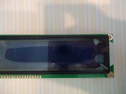 Photo 1.
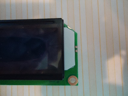 Photo 2.
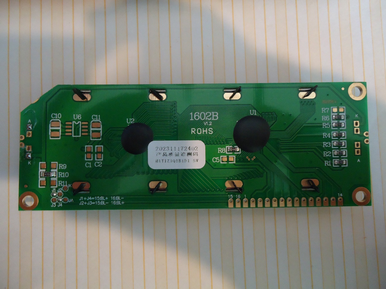 Photo 3.
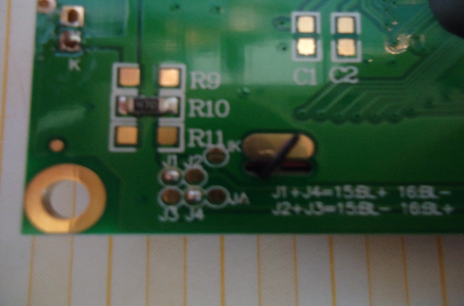 Photo 4.
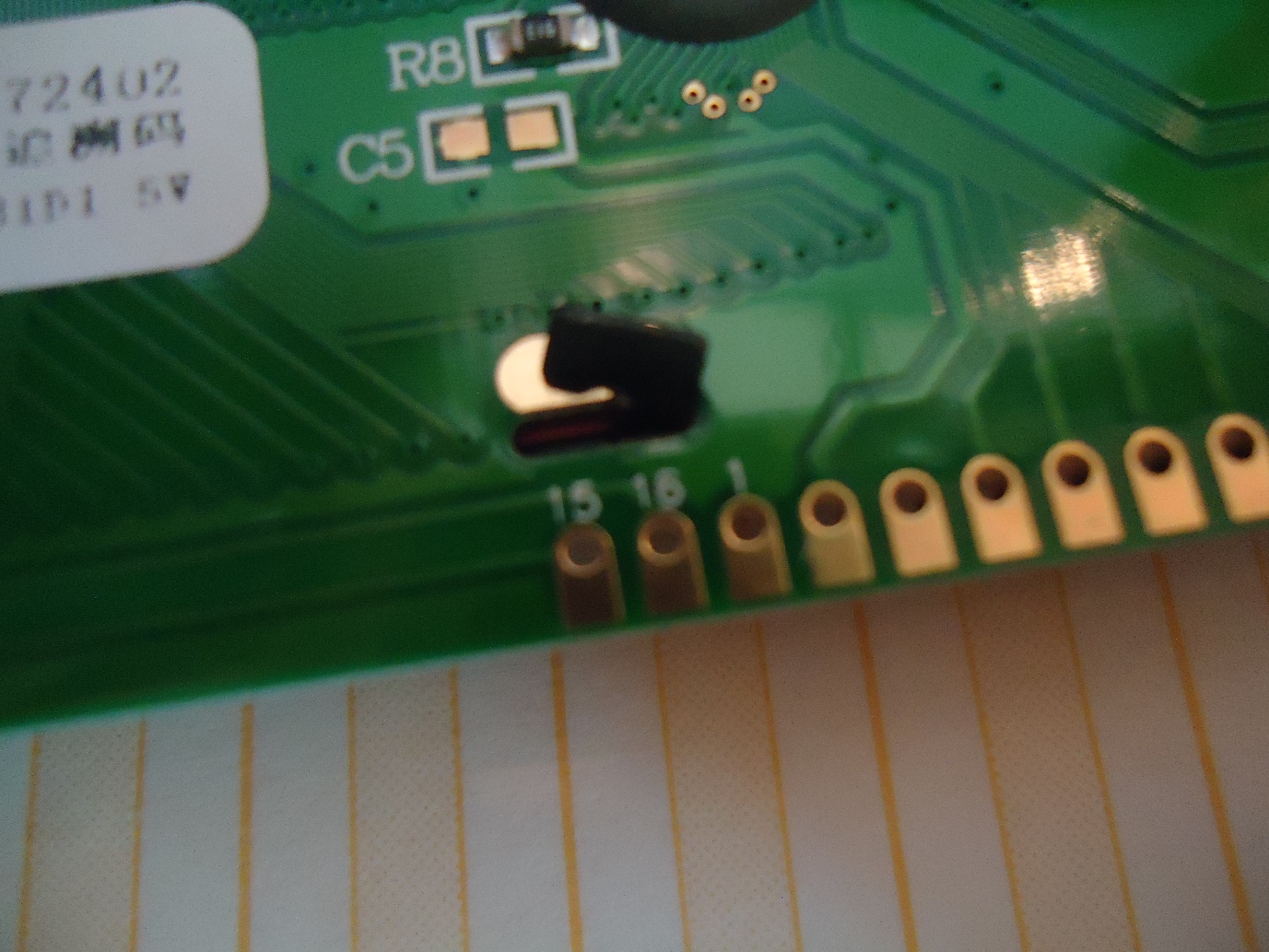 Photo 5.
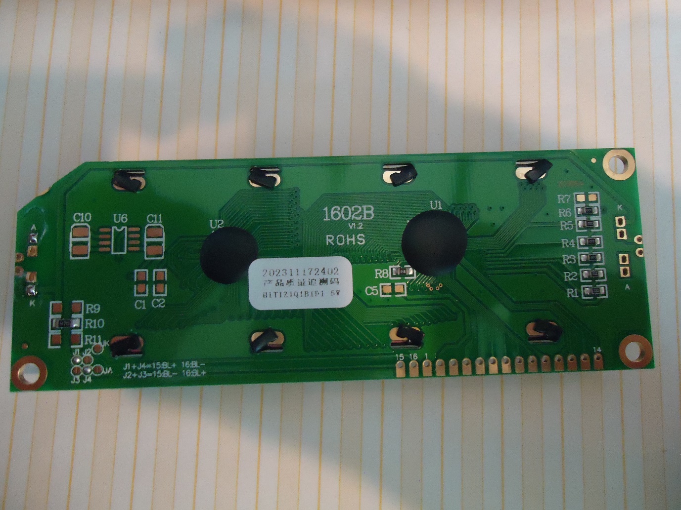 Photo 6.
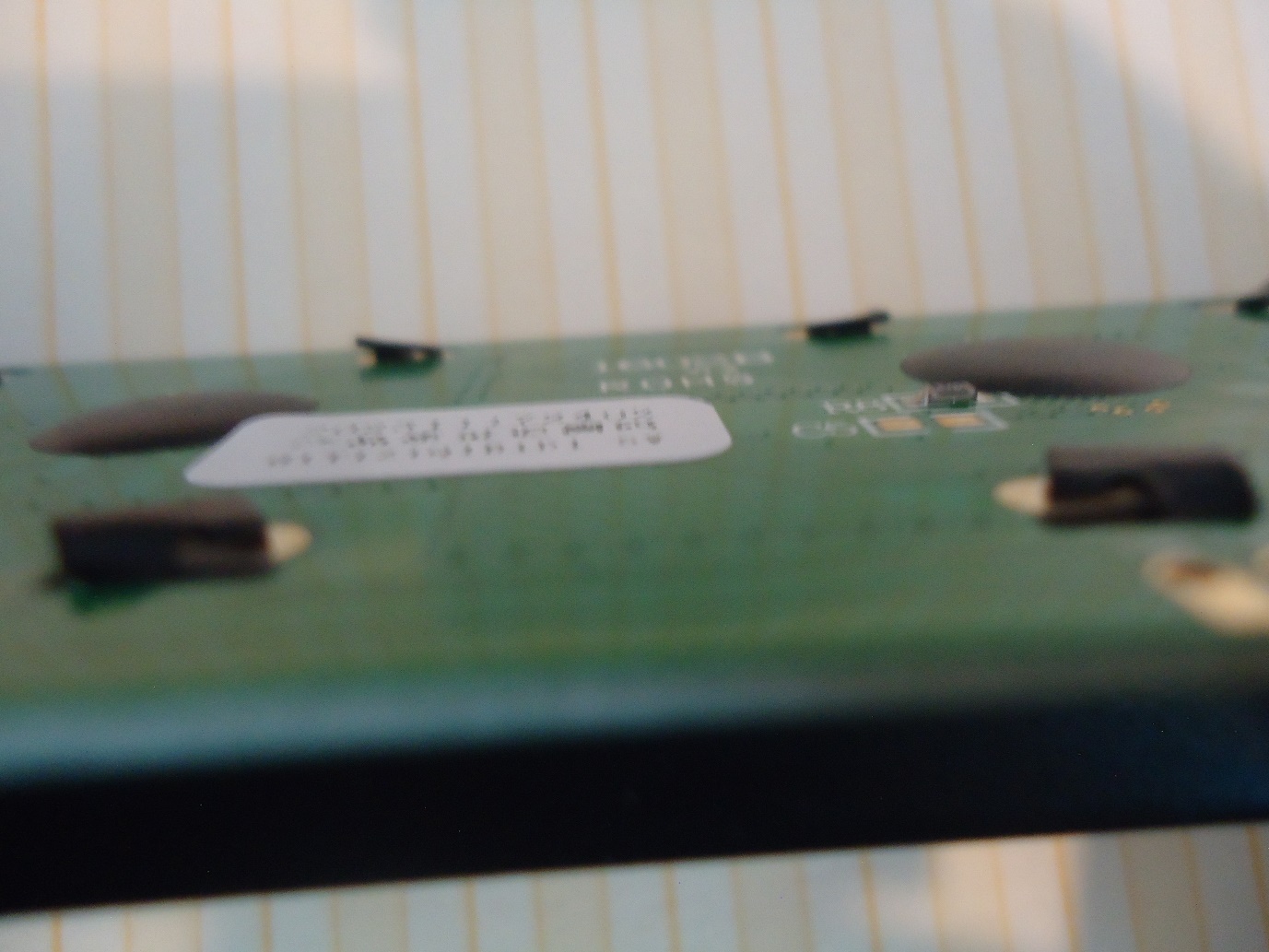 Photo 7.
Back to Top-
Photo 7.
Back to Top-