TAIT 8100 VFO
INTERFACE
PROJECT
by Keith Dix ZL1BQE
This VFO interface kit is another kit designed by Papakura Radio Club
member, Keith Dix, ZL1BQE.
Full credit goes to Keith for the design. This VFO kit will plug
into the DB15 connector on the back of the Tait 8100.
These kits are available from David ZL1DK. Cost of each kit is $125.00.
(subject to change)
Email.
You can contact David directly via email on
ZL1DK
Just click on his callsign to email your interest to David.
Please note, I take no credit for this project and please read my
Disclaimer
and you understand it before
continuing.
Description of This Project:
Tait 8100 Series VFO Kit with 99 Memories.
This is a VFO unit that has been designed for Ham use and incorporates
most of those facilities that we would experience with a commercially
built radio from Icom, Yaesu, Kenwood etc... The software has been
designed to take 99 programmed memories.
This VFO unit will ONLY work with either the VHF or UHF Tait 81xx series
radios. You tell it which one you are using, so if you have both version
radios, you will need two of these kits to assemble. One for each radio.
The repeater shift is stored during this initial setup function. 600kHz
for VHF and 5MHz split for UHF.
There are 99 memories all stored in the VFO unit and not in the radio’s
software, which may have only provision for 10 memories.
Features include, scanning, the partial memory list, or any frequency
from that list, or part of the band, or you can adjust the time the
scan function pauses on a signal, and you can cut out noisy signals,
where the scan function would normally pause.
You can adjust the power output level to 1 Watt (X), 5 Watts (L),
10 Watts (M) or 25 Watts (H).
If a DTMF Microphone is connected to the display, DTMF can be added to
your transmission. You will need to check connections to the RJ45, 8V DC
is available on Pin 2 of the RJ45 to supply a DTMF encoder.
If the power is disconnected, the display will also remember the last
settings and reinstate's those settings on restart.
If a headset is used a headphone could be added from J13 to a headphone
socket on the escutcheon connection from the front RJ45 connection.
There is also an 3D printed escutcheon that Robert Patterson, ZL4ROB has
made to clip this kit to the front of the radio to finish off the
project.
If you need more info on the 3D escutheon, you can contact
him via QRZ
Programming the Tait 8100:
To make the interface work, the radio will need to be programmed
Initially to set the I/O ports on the DB15 socket, to send the right
signals to the display board. If you need to do this, see the
"programming info" link below on how to do it.
WARNING: You can do HARM if you don't know what
you are doing, so before you change anything here, seek advice FIRST.
Programming Info
Programming the Memory Channels and General Operation:
Download the manual and follow the operating instructions. Click on
the links below. The latest version is Ver 4.35
You should be running the lastest version.
You can also download the Full Operation Manual, and a Quick Guide.
I have added the latest version 4.35
Updates to the Program
Updates to the program were made, so if you are running version 4.32,
I recommend to upgrade to version 4.35.
To check what version you are running, when you first power up, the
VFO displays the version number.
To upgrade to this version, you will need to contact Keith ZL1BQE direct
or me via this website. He will either flash the your old IC or swop it
over. This IC is on a IC socket so it is easy to remove.
Download 3D VFO Case Front
You will need a 3D printer to print the case.
There are two types, one for a single VFO radio and the other for a
dual vfo version. The dual version would require two VFO kits and two
radio's.
Thanks to Rob ZL4ROB for the designing, of these 3D cases.
Notes on 3D Printing.
The files are in the later format .3mf
When printing either of these cases, print them to have the larger side
up as this will produce a better print. This can be confirmed by having
the writing up the correct way up when viewed in the printer.
Note that the writing is not shown when connected to the radio.
Print at 0.2mm layers and 20%+ infill.
Clicking on either of these links below will download the file direct to
your PC.
Download Single Head VFO Case .3mf file to PC.
Download Double Head VFO Case .3mf file to PC.
If you need .stl files, these would need to be converted to .stl
If you have any problem, please contact me.
Download Manual
You will need to click on the "links" below to download the manual
required.
Download Tait 8100 ver 4.32 Operation Manual to PC.
Download Tait 8100 ver 4.32 Quick Guide to PC.
Download Tait 8100 ver 4.35 Operation Manual to PC.
Download Tait 8100 ver 4.35 Quick Guide to PC.
Home Construction.
For those who are about to start building this kit at home, please
follow this step by step guide and that you read and pay attention to
these instructions, these are to help you assemble this kit.
I recommend that you read through these instructions first before you
start construction, as to pick up tips as you go and make construction
enjoyable.
Main Construction:
Before you start construction.
Refer to the parts list supplied. I would also recommend to read the
instructions below FIRST for construction tips and recommendations
BEFORE you
start assembling this kit.
Also if you need tips on soldering,
please see my
Solder Basics & Construction Tips
for further tips to help with the construction
of this project.
Failure to read these instructions may cause problems later
when the kit all comes together.
Once assembled, and you have any problem or issues see the
Trouble Shooting section below.
Unpacking the Kit.
When you receive your kit, I recommend to open the kit and put into a
click clack box or similar. This is so when you open the kit all the
parts will be in the box and will NOT get lost later.
In the kit is also a anti-static bag containing the 3x IC's U2, U3 and
U4 plus the 5v regulator U1. These are electrostatic sensitive devices
so handle these with care. I suggest you follow the ESD guide lines and
to use a wrist strap when installing these devices. Always leave these
ESD devices in the anti-static bag until you are ready to use them.
Search online for wrist straps for more information on this...
Sorting Components
First, prepare all the resistors as per the quantities in the parts
list, and sort them into there values.
I recommend that you use a
ohm meter and measure each resistor just to make sure you have the
correct value ready to install.
Only remove from the box the components you are going to install.
Construction Tips:
Photo 1. Shows the completed rotary encoder kit.
This kit has 1x PCB, 2x LED's and 1x rotary control and 6x sets of 2
header pins. 2x spacers for the LED's.
First look at photo 1, we are going to install the header pins. These
must be kept straight when you solder them. Insert all the pins onto
the board.
TIP: Using
the main board as a guide, place the main board flat on your work
surface and insert the pins on the board but DO NOT solder these pins to
the main board. This is only to align the pins and to keep the pins
straight while you assemble. Also these black spacers,will stop the
header pins from going all the way through the board and this would
prevent the rotary dial from being installed correctly. If spaced right
you will have just enough of the pin showing for you to solder, and the
rotary dial will be flat on the board when you come to install it.
Solder the header pins to the sub board so the pins are through the PCB
resting on the black spacer.
Now fit the rotary control to the board and make sure all of the legs
are installed through the board before you solder it. See photo 1. as
a reference.
Next fit the spacers to each of the LED's. These spacers have 2 holes
through them for the led pins. Once this is done, be careful and make
sure you fit them in correctly. Fitted one way round the LED is Red,
fitted the other way around the LED is Green. Looking at the LED, You
will notice one leg is longer than the other.
Fitting the LED's.
View the PCB from top side with rotary encoder facing you LED holes at
the top Left LED the long lead goes in to the hole with the round pad
the right LED, long lead of the LED goes into the Hole with the square
pad.
Alternately, looking again at photo 1, the LED top right D2 shows the
longer leg on the right hand side marked long leg. The other LED D1,
the long leg is fitted the other way round. This is very important as
the polarity matters to what colour is displayed.
Fit the LED's as shown in the photo and make sure the leds plus spacer
are all the way on to the board.
Trim the LED legs only once it has been checked.
This part of the kit is now complete and should look like the photo.
(The LED legs should be trimmed.)
Rotary Encoder Control Modification.
This part is found in the rotary encoder kit and this requires to be
modified. It has a small extrusion on the top part to stop rotation
of the encoder when mounted on a panel. (Shown below) This must be
removed as it is not needed.
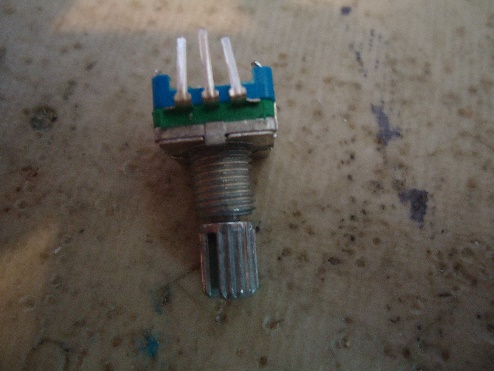 Before.
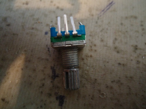 After.
The photo above shows the extrusion removed. A good pair of side
cutters can remove this and a small file for any burrs left. This will
now allow the control to sit flat once the front panel is fitted.
It is a lot easier to do this modification once this board is assembled.
Put to aside for now, this board is now complete and ready to be
installed later on to the main PCB.
Photo 2. Shows the completed version of the push button kit.
This kit has 1 PCB board, 5x tact switches plus buttons and 5x sets of
2 header pins. To assemble this, we will put the header pins on first.
On the PCB board place the board with Keith's callsign ZL1BQE face down
flat on your work surface.
Install each header pin on the PCB with the spacer at the top. See
photo 2.
With the board flat, fit the header pins so they just go into the
PCB, and these header pins will be flush with the other side.
If you don't follow this step, the tact switches will not be flat
on the board when you go to install them.
Solder one side first and make sure the pins are straight, before
soldering the other side. Tip: It is easier to correct and straighten up
the pin with only one side soldered first. It is important these pins
are straight as this PCB will fit onto the main board later.
Do this for all five header pins.
READ THESE NEXT 2 STEPS BEFORE YOU SOLDER THE TACT SWITCHES.
- The tact switch MUST be flat on the PCB.
- Two pins of the tact switch needs to be trimmed before soldering.
Step 1:
First check in photo 2 to see which pins that are required to be soldered
and which 2 pins need to be trimmed.
The pins to solder first of the tact switch are either side of the
header pins. In the photo, you can clearly see two pins of the switch
are trimmed and lower.
When soldering make sure the tact switch is flat by soldering only one
pin first. correct this now if the switch is not flat. If ok, continue
to solder the next pin on the PCB.
Step 2:
You should have only two pins of the tact switch soldered. Cut and trim
the other two pins of the tact switch BEFORE you solder them. This is
so the two pins are even lower and do not touch the display once fully
assembled.
Once trimmed now solder them.
Do this for the other four switches.
If you did not follow these steps above and soldered all 4 pins, then
the display will come very close to the switches and possibly touch and
short out.
Put aside for now, this part of the kit is now complete and should look
like the photo. It will be installed on to the main PCB later.
Display Modification.
Click on this link for the instructions to modify the display.
After you click on the link below, it will open a new tab/window, so
once you have completed the modifications, simply close the tab to
return back here.
Display Modifications
Main Board Construction.
Photo 3. Shows the 1K resistors installed.
Start off by installing all the 1k resistors. (9 in total) These are R1,
R2, R3, R9, R10, R12, R17, R26, R30. Start soldering these in making
sure thay are flat on the PCB. You can install these a few at a time
until all 9 resistors are installed. After soldering, cut off the legs
close to the board.
Photo 4. Shows the 1K and 10K resistors installed.
Next install the 10K resistors. (11 in total) Again you can install and
solder a few at a time until all 11 of the 10K resistors are installed.
These are, R4, R7, R14, R15, R19, R20, R21, R22, R23, R24, R42.
When soldering these in and make sure they are flat on the PCB as you
go.
Photo 5. Shows the 1K, 10K & 4k7 resistors & Diode installed
Next, do the same for the 4K7 resistors, (10 in total) these are R13,
R18, R32, R33, R34, R35, R36, R37, R38, R39. Install the rest of the
resistors, there are two 2K2 resistors R5, R6. Then install two 47K
resistors R25, R27. Next Install two 100K resistors, R40 and R41.
Now Install the single value resistors, again making sure you install
the correct value resistor, as you can easily install the wrong value
resistors here, hence this is why it is best to measure them first.
Install the 100ohm, R28.
Next 33K resistor R29, This resistor is
listed as 39K but use the 33K resistor supplied.
Next install the
300K resistor R31, and the last resistor, the 1M resistor R8.
All the resistors should now be installed, as shown in Photo 5.
Note
R25 and R27 are not installed at the time this photo was taken.
Install the diode D1 making sure you get it around the correct way.
Looking at the diode, it shows a line at one end. This is the cathode
end of the diode. On the PCB, find D1's location and insert the diode.
The cathode is marked k. If unsure ask before soldering.
Photo 6. Installing the Capacitors
You can install these capacitors in any order. I would recommend to sort
them out into each of the values first, ready to install. I installed a
few at a time, soldering one leg first, then checking to make sure they
are fully seated and upright and trimming the legs once soldered.
Sorting the capacitors out first makes it a lot easier as you have now
identified what the value is and the quantity of each value.
It is good practice to install the same value capacitors as you go just
like you have done for the resistors.
I started first with reference C6 and C7, both 18pF.
Next to install I did C2 and C5 both are 10uF, and these are marked 106.
I next installed C1, C4 and C8, the 3x 1uF, these are marked 105.
next to install are the nine .1uF's, Reference C3, C9, C10, C11,
C12, C13, C14, C15, and C16. These are marked 104 on them.
With all the capacitors now installed, at this stage, your kit should
now look the same as photo 6
Photo 7. Installing the rest of components
Install the fuse F1. This needs to be bent over, see Photo 7. Next
install U1, L7805 5v voltage regulator. This needs to be bolted down
using the plastic nut and bolt. Install U5, MC78L08 8v voltage
regulator.
Check and install the correct way round, bending the
middle leg slightly, so once installed it lines up with the flat side of
the regulator to the flat side marked on the PCB. Push this down as far
as you can.
See photo 7.
Install the 6 transistors next. Q2, Q3, Q4, Q5, Q6 and Q7. These are all
BC547's.
On the PCB you will see the outline of the transistor. It shows a flat
edge and has 3 holes. You need to bend the middle leg slightly to fit
into the top hole and fit the transistor with the flat side, the same
on the PCB.
Install Y2 crystal, 3.57945Mhz. this is a through hole crystal.
Next install the SMD crystal Y1, 29.4912Mhz. When installing this,
solder one pad first, then align the crystal in the center of both pads.
Heat up the side you just tined, this will join the crystal and hold it
in place while you do the other side. Be careful not to apply too much
solder here as you do not want to get any solder on the crystal.
Install the 10K trim pot RV1,
Install the IC sockets U2, U3 and U4. Make sure these are
sitting flat when you install them.
When doing the IC sockets, solder one pin first, then solder the
opposite corner that you just soldered. Check it is still flat. Now
solder the other pins as the IC will no longer move. Do this for all 3
sockets. We will fit the IC's in once the main board is fully assembled.
Next install the multi resistor array RN1, (8x10K) Make sure this
is installed the correct way around. There is a dot which is pin 1.
Install J1, the 16 pin connector for the DB15 cable.
Install the J13 4 pin connector.
You now should have all components installed except for the RJ45 socket.
Do not install this yet as it is installed in the last steps.
Assembly of the display and sub boards to the main board
Photo 8. Installing the Header Pins
Fit the header pins onto the main board and push them in half way
through the board. as shown in Photo 8.
DO NOT solder these pins
to the main board. The push fit can be quite tight as the pins push
through the first time, carefully wiggle as you push them. The reason
why they are not soldered is that the length needs to be adjusted when
they pass through the display board, AND the tight push fit will allow
the display board to be removed in future if servicing is required.
Photo 9. Installing the Display on to the Header Pins
Make sure the display has been modified before fitting.
Next fit the four brass stand offs to the main board as shown in photo 9.
These brass stand offs will hold the front panel board once installed.
Next fit the display board onto the the header pins. Place the three
plastic spacers between the display and main board and then fit the
longer bolts through the display and fit the nylock nuts to hold down
the display. Tighten down but do not over tighten.
The header pins will be too long when fitted to the display as you can
see in photo 10.
Photo 10. Showing the Display Installed on to the Header Pins
As these pins are too high and not yet soldered, it is easier to push
the header pins back down from the display side to almost flush with the
display, ready to solder.
Photo 11. Showing the Display's Header Pins ready to solder.
You can see in photo 11, the header pins have now been pushed back down
near flush on the display board allowing enough of the pins ready to be
soldered.
Photo 12. Soldering the Display Header Pins.
You can now
solder the header pins to the display PCB board top side
ONLY. There is no need to solder on the underside of the display
board as the connection is joined both sides anyway.
Turn the two boards over. The excess header pins will now be sticking
out of the main board. As noted in Photo 8,
DO NOT SOLDER THIS SIDE
TO THE MAIN PCB. By not soldering this end, it is to allow the
display board to be easily removed in future.
The tight push fit mimics a plug and socket connection and is sufficient
for the voltages and current to get through. Trim the excess pin length
to around 5mm sticking out from the main board. Once again remember
Do not solder these pins to the main board.
Making up the Ribbon Cable Lead.
Photo 13. Shows the 16 Pin Ribbon Cable.
In Photo 5, you can see pin 1 of the 16 pin socket. (Bottom LHS) Once
you fit J1, you can no longer see pin 1, but see photo 15 as this shows
the correct way round to fit the lead.
Fitting the wires to the Ribbon Cable.
On the cable, pin 1 is marked with the red trace.
As there are only 15 wires required on the DB15 connector, we need to
peel back the 16th wire and cut it off so it will fit the IDC connector.
You will need a small press like a mini vice to squash the connector
together.
Take care and DO NOT overtighten, otherwise you will
damage the connector. Photo 13 shows the lead cut and the correct way to
dress the ribbon cable onto the connector.
Testing the Display.
Before you continue to solder the rotary encoder PCB and push button
assembly in place onto the main board, you can power up the VFO using
the ribbon cable to your radio. This test will check if the display and
backlight is working Ok. You may need to adjust the trim pot RV1 for
contrast to light up the display. This adjustment will be almost at
maximum adjustment.
Any problems with the display or no backlight at this stage, Scroll down
to see the
Trouble Shooting section for details on how to fix.
Repeat this test (if necessary) and ONLY PROCEED, to the next step if
you see the blue backlight lit and the display is showing information up
on the screen.
Display Working
Continue to fit the rotary encoder PCB and push button assembly onto the
main board.
Photo 14. Fitting the Push Button PCB and Rotary Control PCB.
Fit and insert the button assy and rotary encoder PCB onto the main
board, before fitting the front panel. Do not solder these pins yet.
Align these header pins through on to the main board and now fit the
front panel.
Fit the display panel.
With the Display board and push switches fitted, fit the front panel
with the four screws.
Adjust the push buttons to your desired height and so you have the same
height for all the switches and solder only one pin first, on the left
hand side and one pin on the right hand side and finally one pin in the
middle. make sure all the push buttons are working and adjust if
necessary. Check that none of the push buttons are sticking, before you
solder the rest of the header pins of the push button assembly.
Carefully align the LED's through the front display and now pull up the
rotary encoder control so it is flush to the front panel.
I have already mentioned about cutting off the locating lug on the
rotary control and if you have not done this yet, this lug will cause
the control not to sit flush up against the front panel.
If you have done the modification, so the rotary control sits flush up
on the front panel, solder one of the header pins to the rotary control
board to the main board.
Check that the control is still flush up on to the front panel and once
ok, solder the rest of these header pins and trim the excess.
Photo 15. Completed PCB Component View.
This photo shows the completed PCB with all components populated except
for J3 the RJ45 connector. This will be the very last step to install
once the front panel is on and the window has been fitted.
Fitting the Window to the front Panel.
The display will still have the protected film over the display.
Do not remove just yet. You will need to make the window fit on to the
display front.
On a flat surface, size up the window and push in to the display.
It does need to be a tight fit, however if it does not fit in at first,
don't force it.
You may need to sand it down on the
edge that is oversized.
Not all the display windows require you to do
this and if it does, it will not need much to take off so be careful on
this next step.
To do this get some sandpaper and lay on a flat surface. Holding the
window, start filing the oversize edge, taking off a very small amount
at a time, checking each time you file off.
File each edge of the window until it press fits into the front panel.
Once the window fits in nice and tight, clean off any fingerprints from
the window, remove the front panel's 4 screws and remove the front panel
so you can now remove the protective film off the display. Refit the
front panel, then fit the RJ45 through the front display. This should
fall into place straight onto the board. Check before you solder, that
all the pins are into the board. Solder J3 once all is OK.
As this project is now fully assembled, you can now start to program the
radio.
Keep following the steps below and the link to download the
user manual to program the radio is found near the top of this article.
Ready to Turn On and powering up for the first time
Before you turn on...
See the troubleshooting section below if you encounter any issues.
Blue Screen only, No Text on Display
For the first inital power up, you may have only a blue screen with no
text. If you encounter this, then by adjusting RV1, on the main board
will bring up the text contrast. The adjustment of RV1 will almost be at
maximum.
External Speaker
The radio will need an external speaker as the internal one was on the
original front panel and is no longer available.
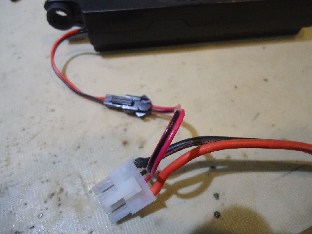
The external speaker output is the two unused connections between the
power cable plug.(shown in the photo below)
If you do not have the plug and socket shown below, then an alternative
option is to use a inline 3.5mm mono socket on the speaker lead.
It is recommended to fit a plug and socket on your speaker lead as a
potential problem I see is the speaker is a balanced output and if any
lead is shorted to ground will damage the radio it would be good to have
a speaker with plugs on it. This means if you disconnect the speaker
there are no bare wires so this will prevent any damage mentioned above.
If you want to know more information or are interested about balanced /
unbalanced speaker outputs, see below.
If you were building this kit with the Papakura club, there were
speakers offered with the plug and socket, if you require a speaker,
there may still be a few left. The speaker does NOT come or supplied
with the kit if you have purchased online. Extra postage would be
required to send, but have limited stock on request.
 Speaker Connection.
The speaker pins, required for the speaker connection are M1561TL.
This is the Molex number.
Photo 16. Shows the 1st Time start up.
When you get to this stage, you will need to select what version radio
you are using. VHF or UHF
Press the button marked A for VHF and B for UHF.
Once selected you then need to press B to accept your choice.
Press button E to exit for no change.
Once you have selected A or B the radio will power off. Turn it back on
by pressing the rotary control knob for 3 seconds.
Photo 17
This photo showing the radio's display,
Top line is frequency and
power level X is Extra Low power (1 Watt)
Line 2 is signal strength in dBm
Photo 18. Shows the parts list
You can print this out if needed. Click on the link above the parts list
or print or save a copy.
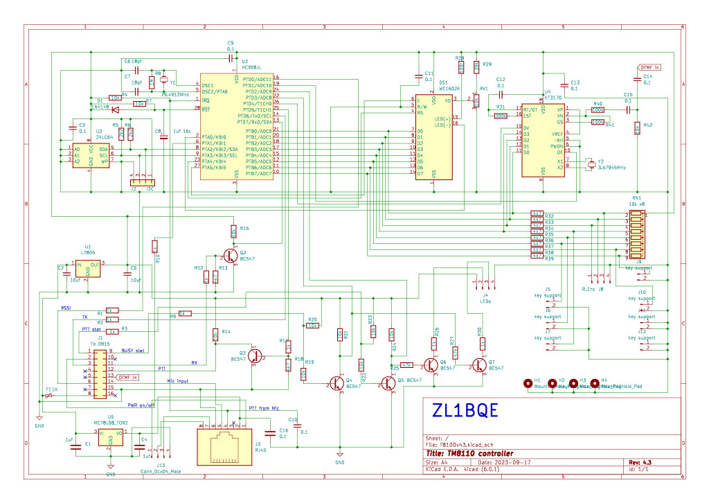
Photo 19. Shows the schematic diagram
This is the circuit diagram of the VFO Controller. Click on
the diagram or the link to show an enlarged circuit diagram. This will
open in another tab. simply close the tab when done and you will return
back to this page.
Balanced Output & Unbalanced Output Explained
If interested, here is some technical background on why you need to be
careful with audio circuits out of radios:
Unbalanced outputs – Most devices you use have what is known as
single ended or unbalanced outputs. An unbalanced output has a Ground
pin and a Signal pin. That means you can plug this type of output into
an external amplifier or other device that has power attached with
possibly a common Ground (negative) between the radio chassis and the
other device. This is OK for most consumer audio equipment but can be
problematic with radios as RF can circulate through the Ground
connections via a ‘Ground Loop’.
Balanced audio output – As the Tait uses a Balanced Audio Output
it avoids the Ground Loop problem. So, if you wish to connect the Tait
audio output to anything other than a standalone, insulated speaker, you
must use a transformer or capacitive coupling between the Tait radio and
the other device to isolate the audio amplifier in the radio from
Ground.
If you don’t, the radio circuitry may be damaged.
WARNING
You can do damage to your radio equipment, so before you do anything
or if you are unsure about what you are doing, ask for some guidance
FIRST.
Some more information – There is a lot of information
out there on the internet e.g. Check out this link below.
Balanced vs Unbalanced Connections.
PLEASE NOTE:
I have done my best to make sure this project goes together smoothly.
If you see any mistakes or I have missed a step or it is unclear to
please email me and let me know and I will add/edit or advise.
Trouble Shooting
As these are not in any order, please read all the trouble shooting tips.
No Sound
The radio will need and external speaker as the internal one was fitted
on the original front panel. This is no longer available.
NOTE: It is recommended to use a plug and socket for the external speaker
connection. Do not just use bare wires as if these wires touch or short
out, it will do damage to the radio. If you are not using the speaker
with the plug and socket mentioned above, then you can use an
alternative 3.5mm inline socket.
The connection for the external speaker is on the unused connections on
the power cable plug radio end.
The speaker pins, required are female M1561TL.
This is the Molex number for the pin. Fit an inline plug and socket on
the other end of the cable so that it will make it easier if you want to
remove the speaker.
Errors on Power Up.
Tait VFO 1st time power up
If the backlight is on but nothing displayed adjust the contrast control
on the back of the PCB to show initial display If the display shows
“Com Error” on 1st power on,
1. Power off by pushing and holding the rotary control knob
2. Power on by push and hold the DTMF button
3. Usually push button VFO for VHF and then 1MHz button for active
Volume control
The display will go off then power back on by pushing rotary control
knob this will reset radio to some defaults you will need to setup all
settings in the setup menu (Push and hold REV button to enter setup menu)
This error is due to the EEPROM contents set to “55” it should have been
erased which would set contents to “FF”
If EEPROM has been erased 1st power will go directly to VHF/UHF selection.
Refer to photo 16 to program the radio for VHF/UHF selection.
Once selected you then need to press B to accept your choice.
Blue Screen only, No Display
If you only have the backlight on, and showing a blue screen with no
info up on the screen, when you 1st power it up, you will need to adjust
RV1 the 10K trimpot. This pot should adjust the contrast up and start
showing the text up on the screen once you start turning the trimpot.
This adjustment will be almost at maximum adjustment.
No Blue Backlight.
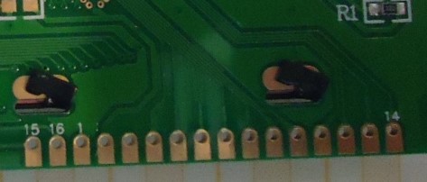
If the Backlight is not working then check the voltage on pin 15 of the
display, this should have 5V then check pin 16 should be 0V.
(Pin 15,16 are located towards the center of the PCB. See picture below
.)
 Display Pin Numbers
Once the display board is running with some characters on the display
although very dim the voltages on the display should be 5V on pin 15 and
0V on Pin 16. If that is correct then the next thing to do is check the
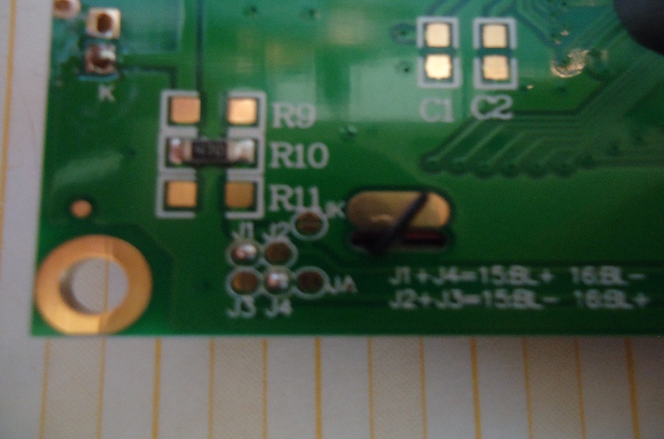
links and if the backlight is still not working, then first check to see
the links are on J1 and J4. If correct try changing the links over to
the other combination. See photo below to change the links.
 Links Changeover
Only do this if you have no blue backlight.
links, 1 and 4 are correct links, BUT have found that some Displays
have the backlight diodes incorrectly assembled with the backlight
diodes reversed and if that is the case then links J2 and J3 should be
shorted J1 and J4 open.
NOTE
Only 2 link combinations should be connected at any ONE time.
J1 and
J4 linked with J2 and J3 open.
Pin 15 BL +5v, Pin 16 BL 0v
or
J2 and
J3 linked with J1 and J4 open. Pin 15 BL 0v,
Pin 16 BL +5v
Next Project Night.
Please go to the Papakura Info Page for further updates.
Papakura Radio Club Info Page
73 de Rob ZL1RJS
Latest Information.
As this has been a club project, some members have now completed the
construction of this project, and is fully working.
This is a step by step info guide, but if you are not sure of any of
the steps, then please ask for help and for now, please STOP and DO NOT
go any further until you are clear on what to do.
This is to ensure assembly of this kit is done correctly.
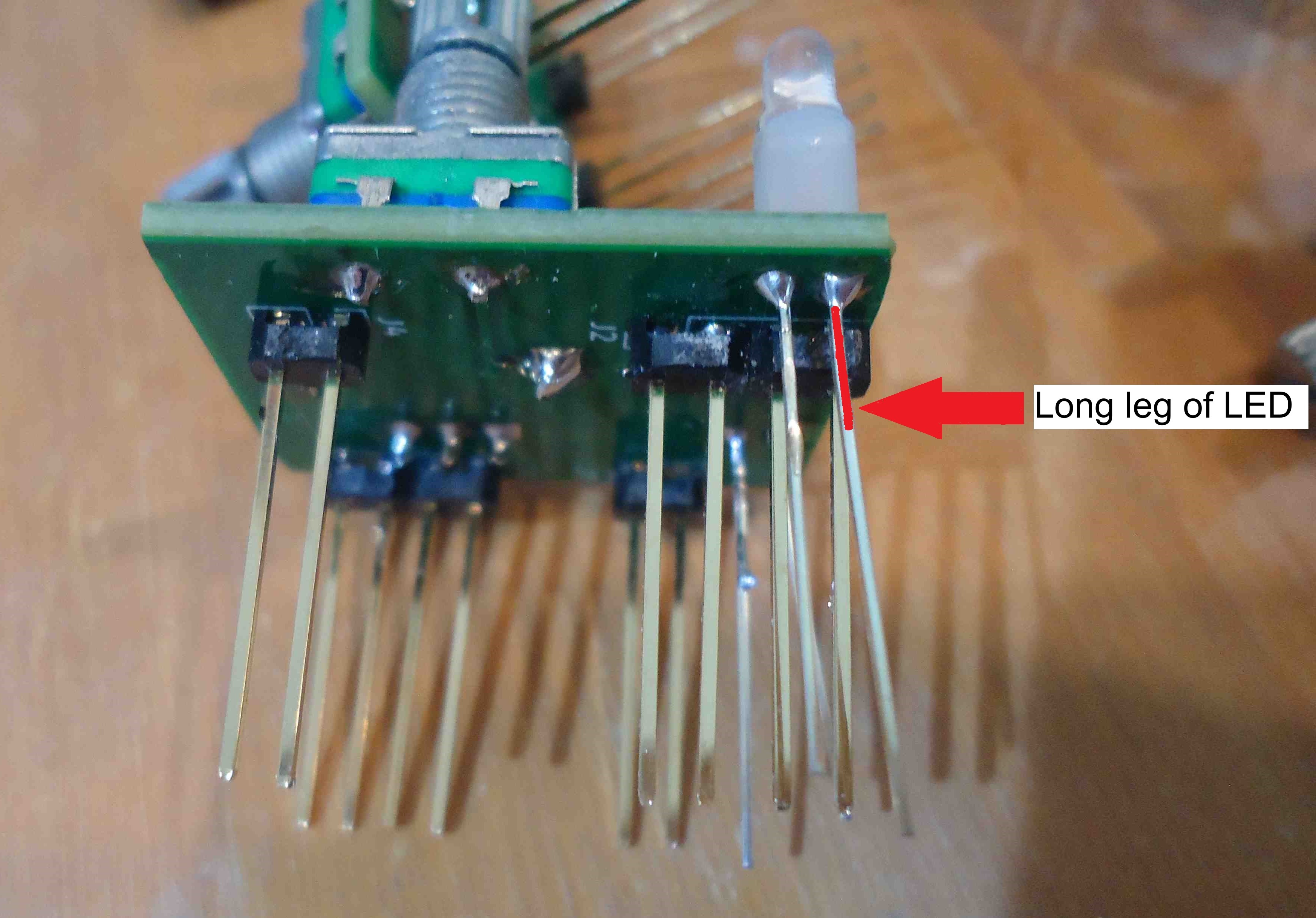 Photo 1. - The Completed Rotary Encoder Kit.
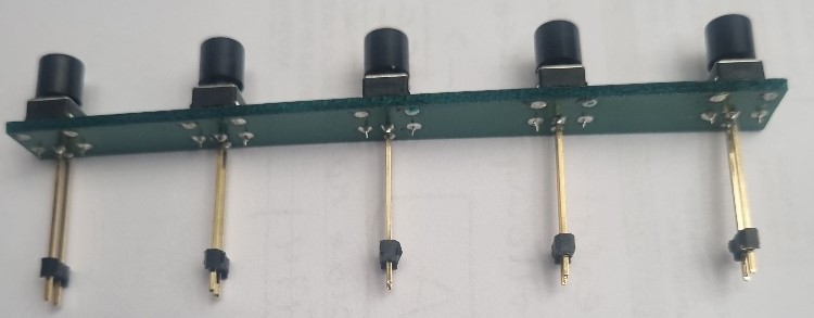 Photo 2. - The Completed Push Button Kit.
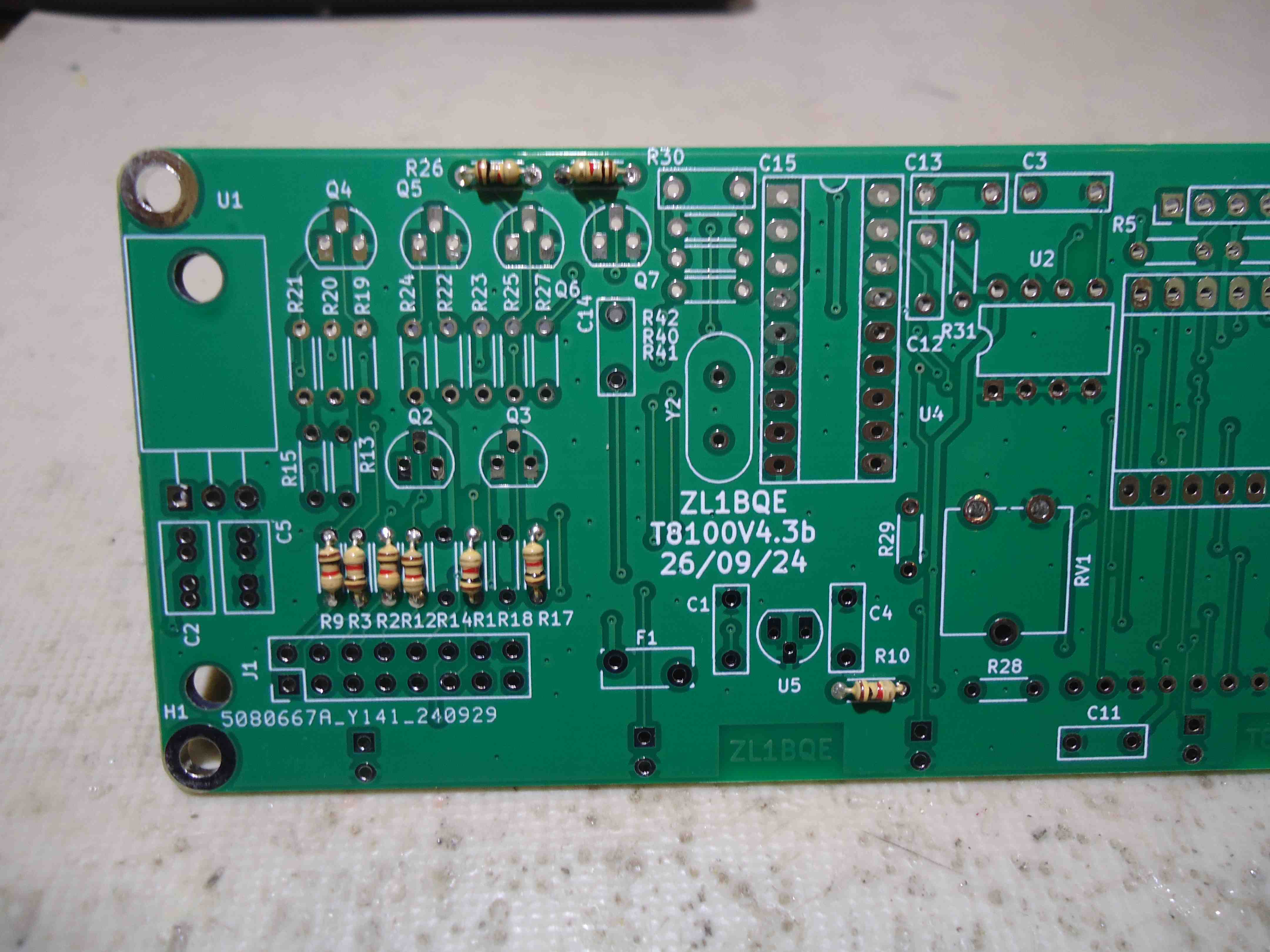 Photo 3. - All the 1K Resistors Installed.
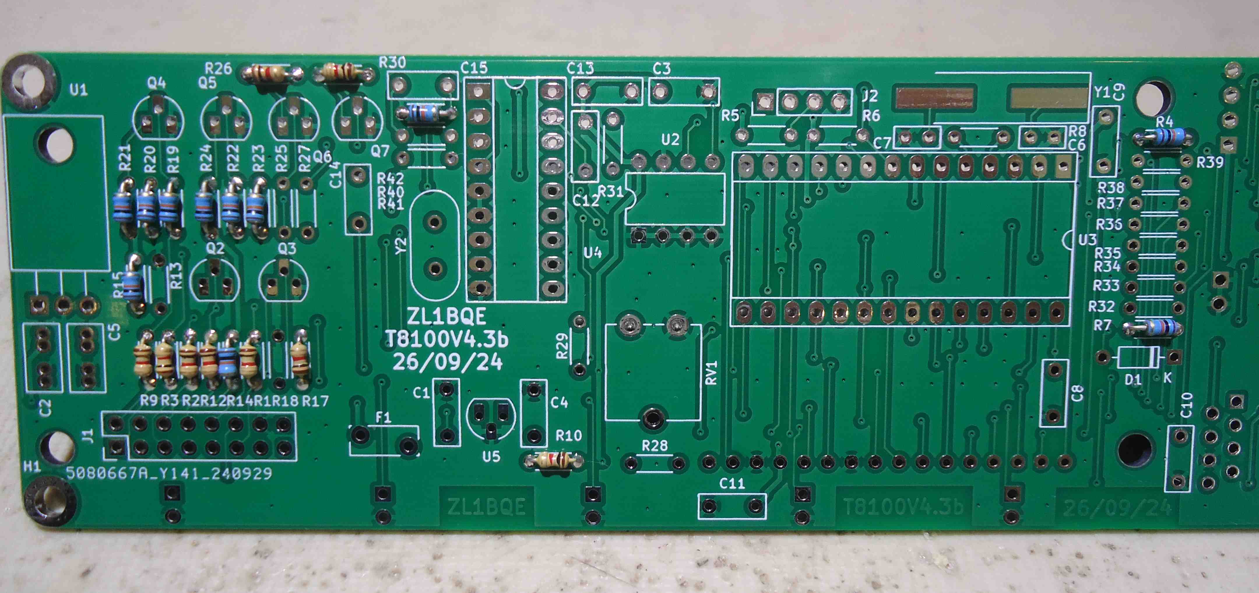 Photo 4. - All the 1K and 10K Resistors Installed.
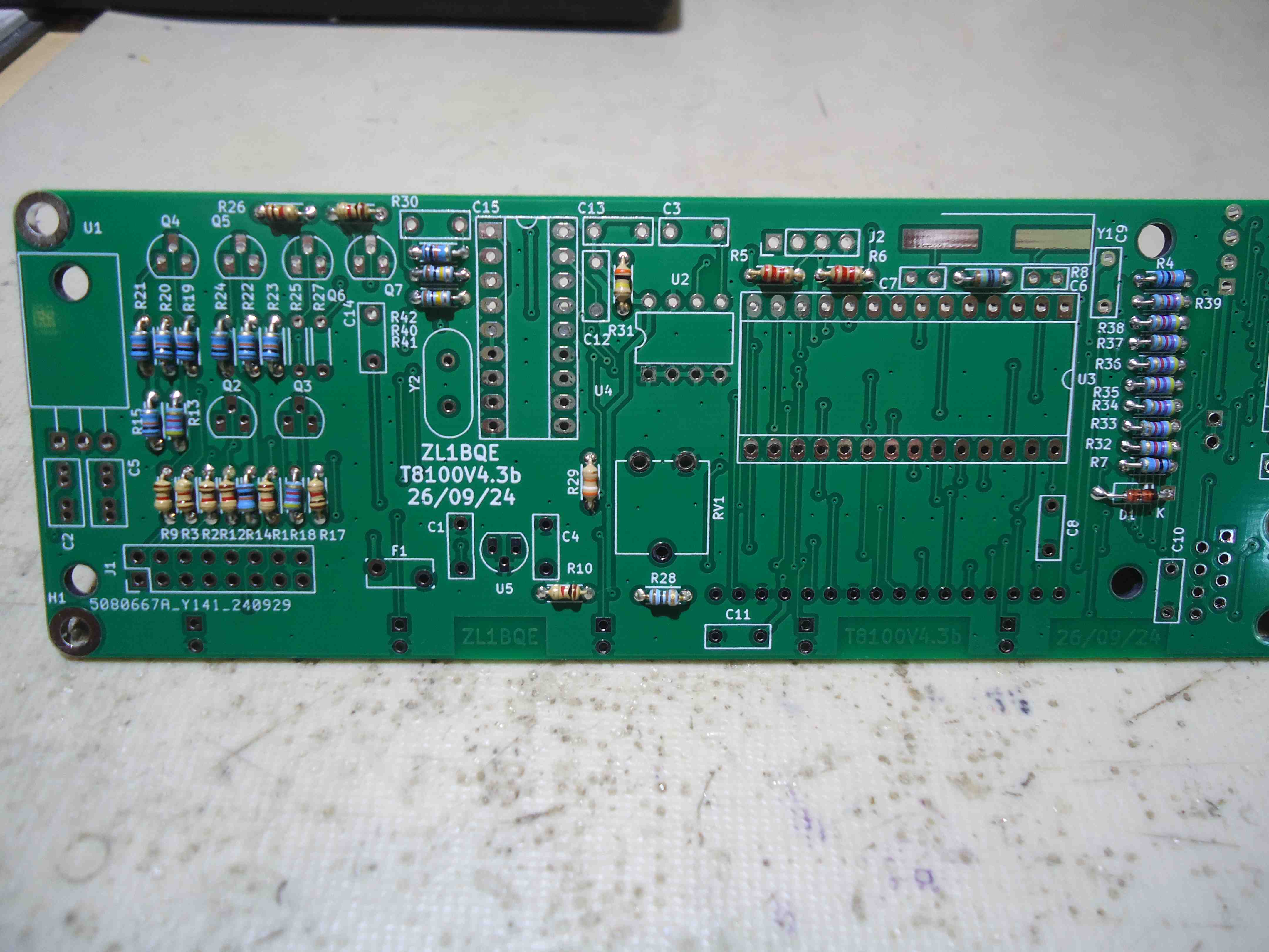 Photo 5. - All resistors Installed (except R25,R27)
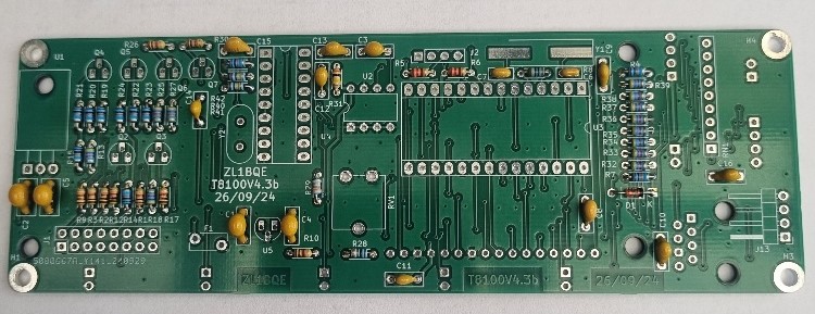 Photo 6. - Resistors and Capacitors Installed plus Diode D1
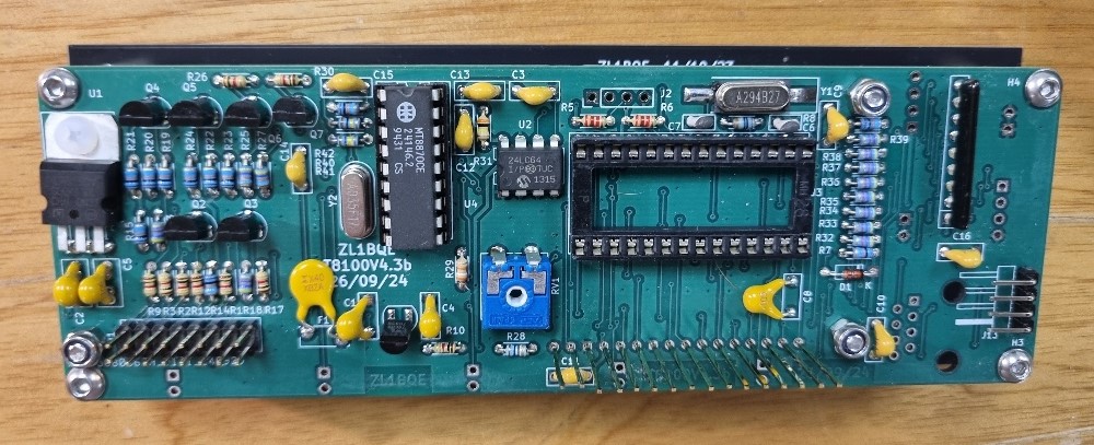 Photo 7. - Rest of the Components
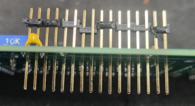 Photo 8. - Header Pins Install
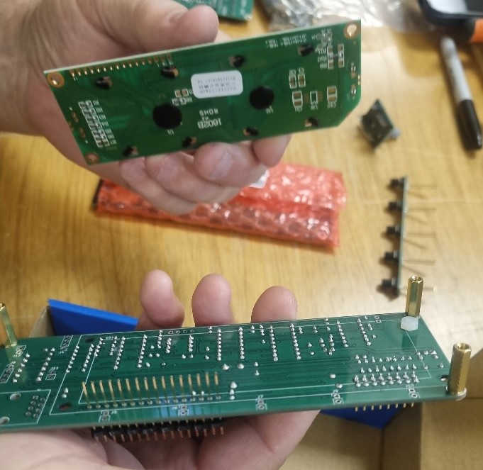 Photo 9. - Fit the 4x Brass Spacers and Display
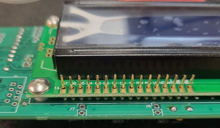 Photo 10. - Installed Display and high header pins
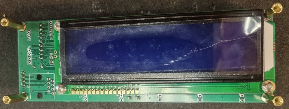 Photo 11. - Pins pushed down, Ready to Solder
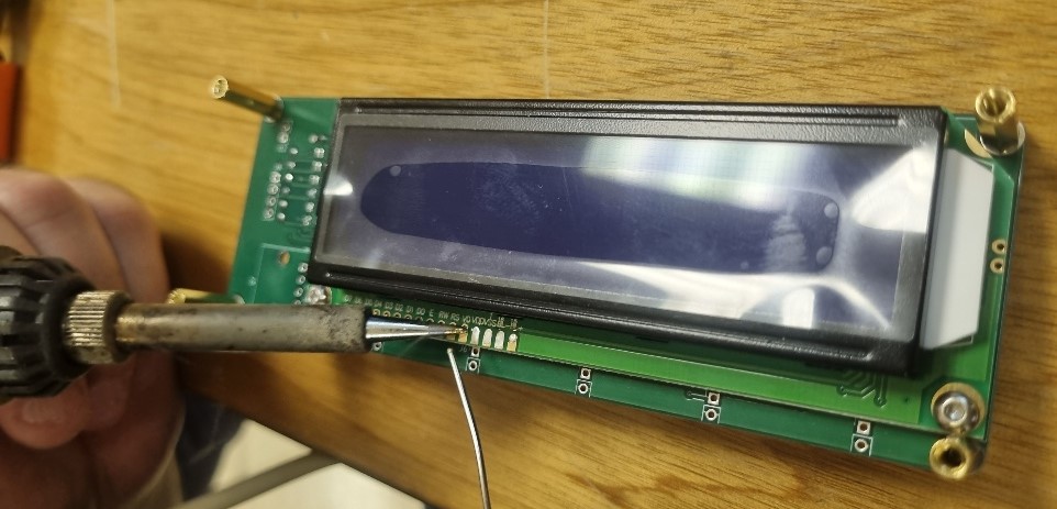 Photo 12. - Soldering The Display
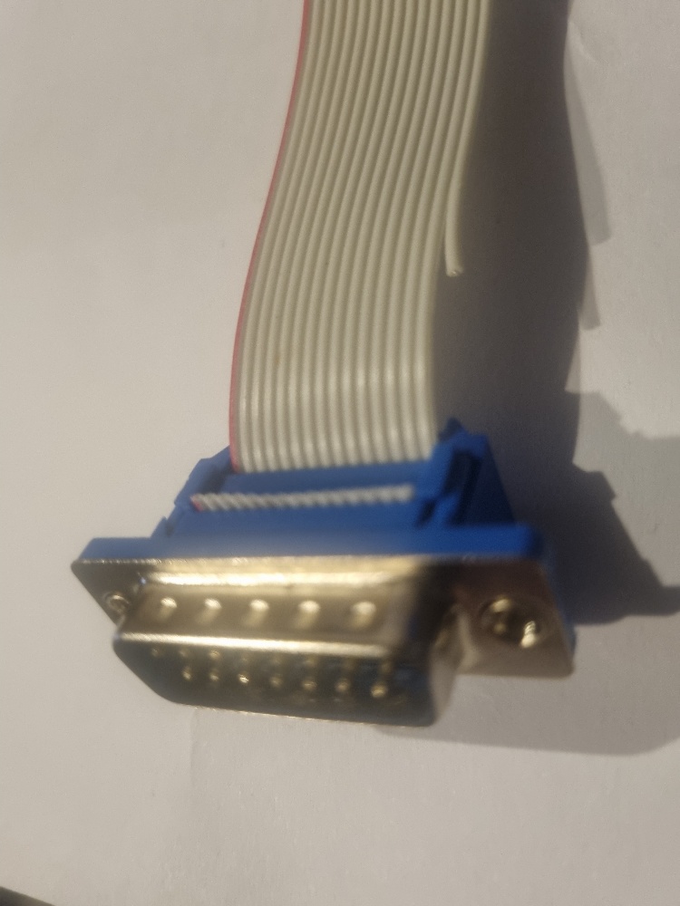 Photo 13. - Shows the 16 wire Ribbon Cable with only 15 Wires Used.
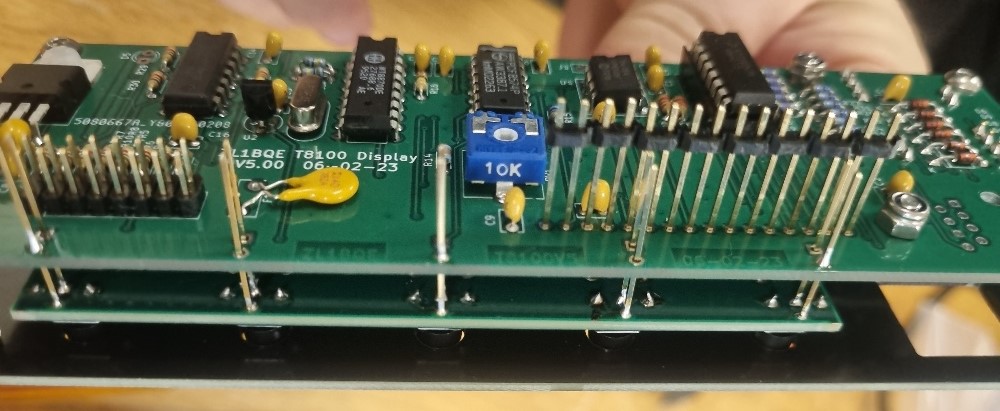 Photo 14. - Push Buttons Installed
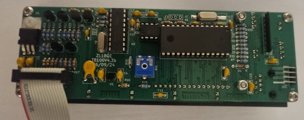 Photo 15. - Completed Component View .
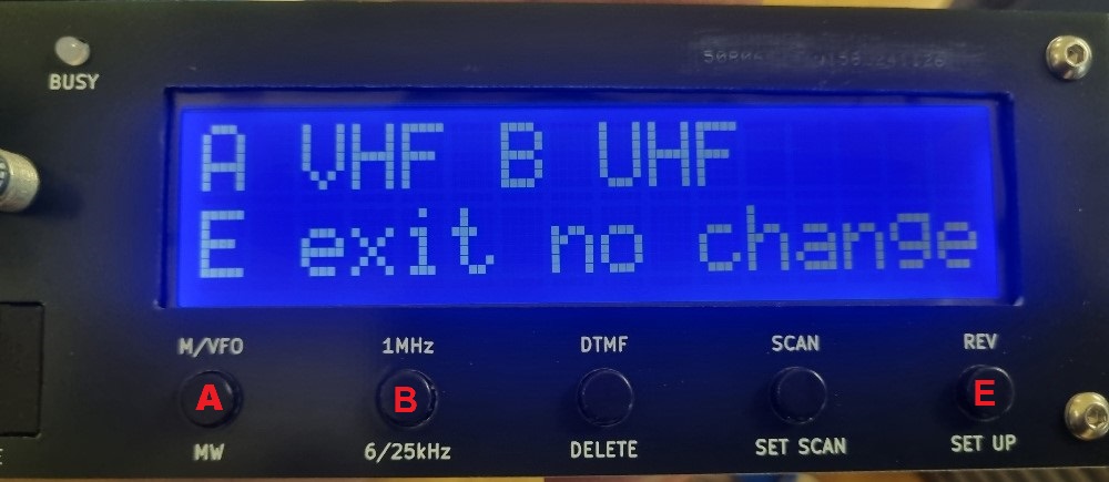 Photo 16. - Setting Radio VHF or UHF
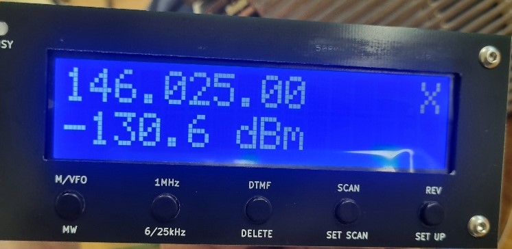 Photo 17. - Frequency Display and power level X (1 Watt) Signal strength in dBm
 Before.
 After.
