USB Radio Interface
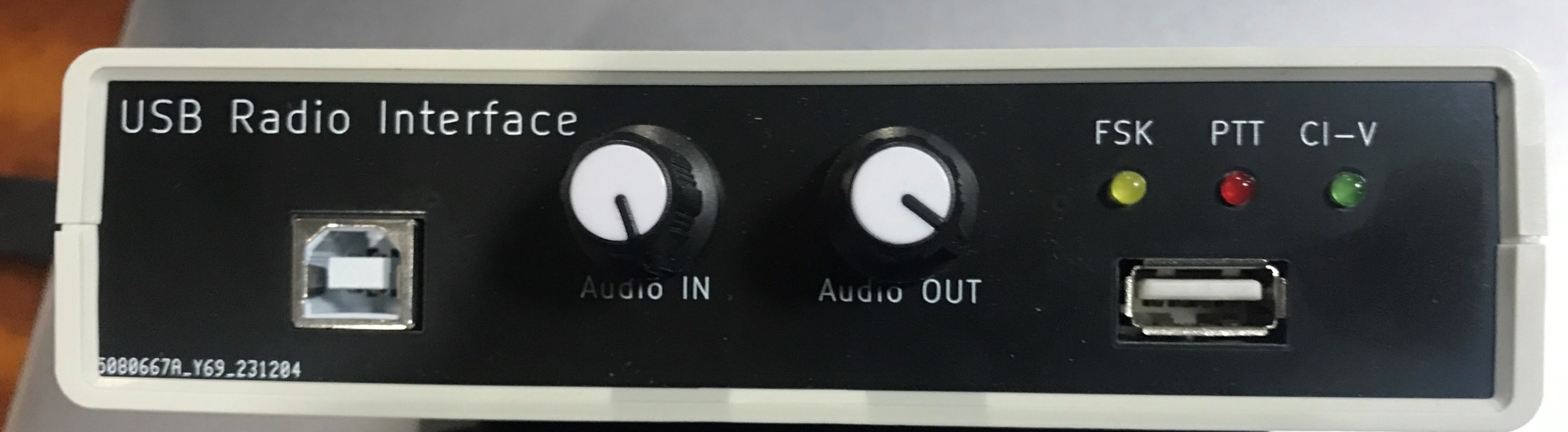 Photo 1.
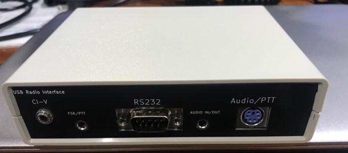 Photo 2.
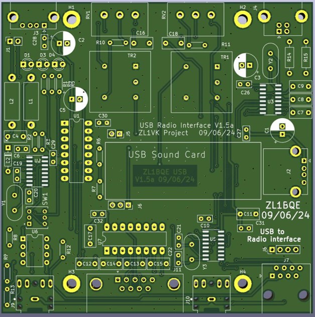 Photo 3.
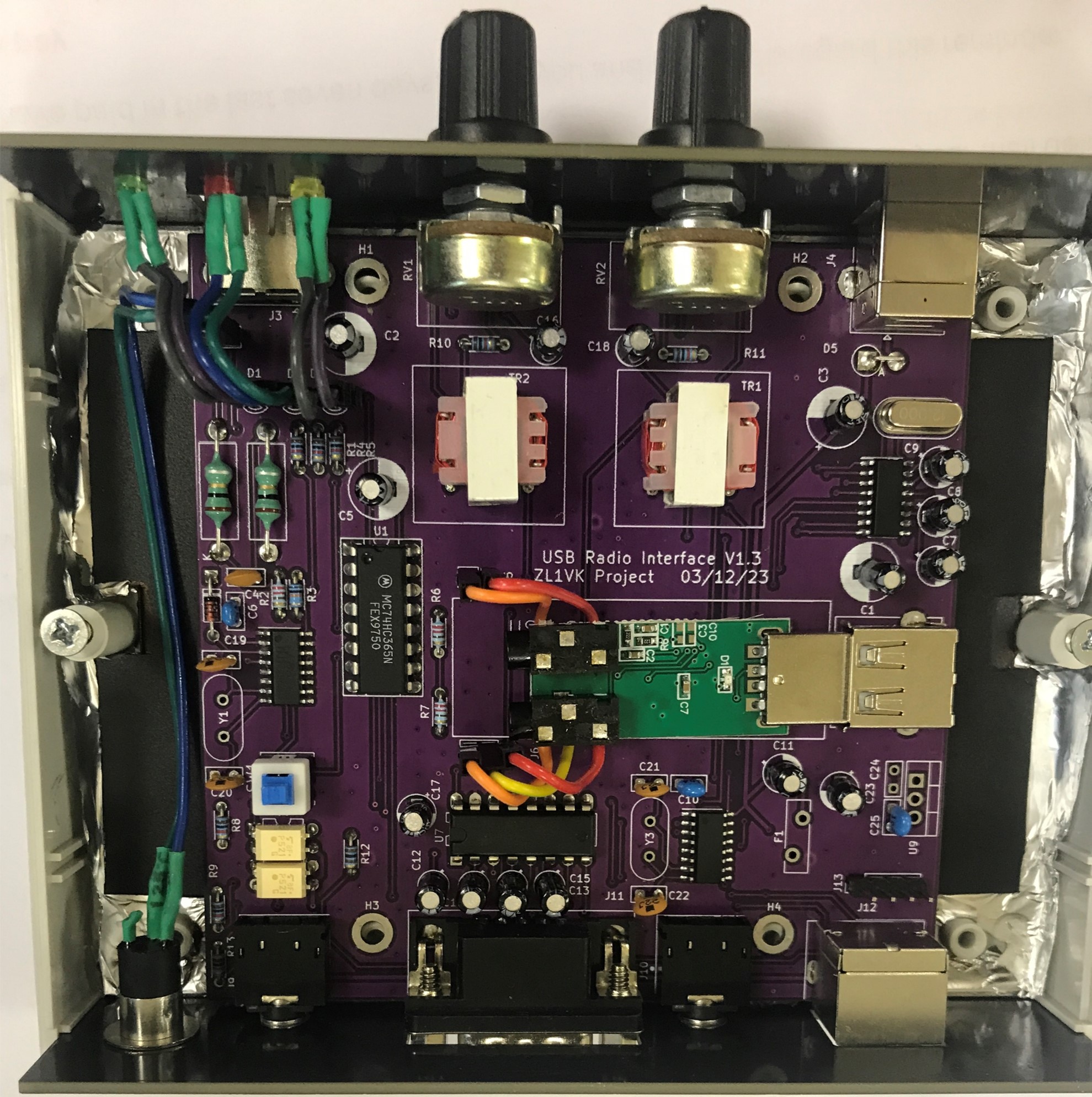 Photo 4.
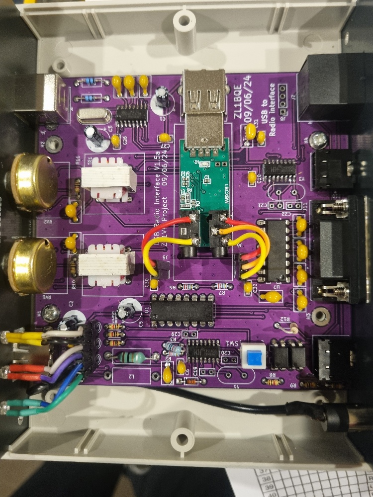 Photo 5.
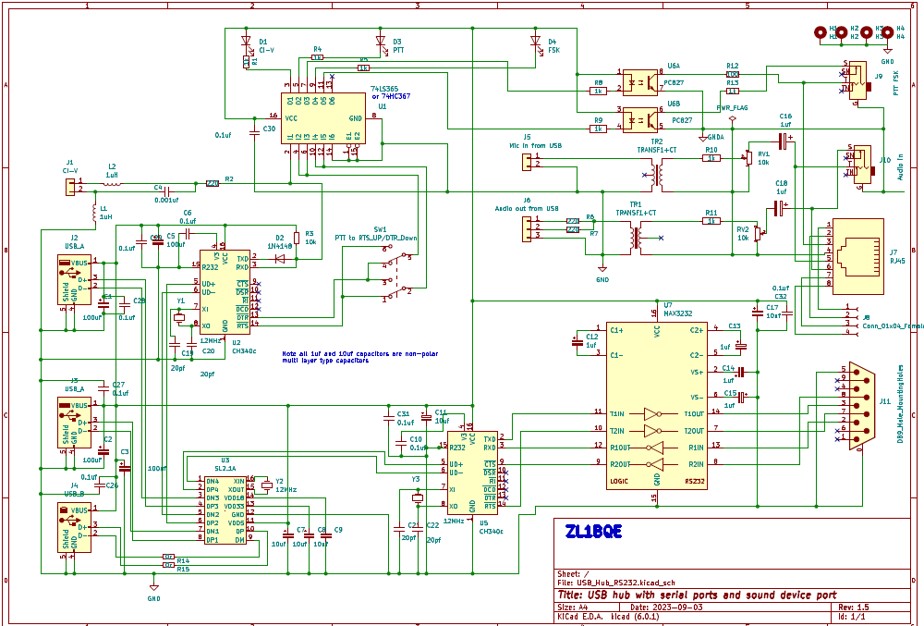
Schematic diagram of the Interface. Click to enlarge on the image above or here
List of Parts
List of PartsBack to Top
Photo 1.
Photo 2.
Photo 3.
Photo 4.
Photo 5.
Schematic diagram of the Interface. Click to enlarge on the image above or here
USB RADIO INTERFACE PROJECT
by Keith Dix ZL1BQE
This USB radio interface kit was made and designed by Keith ZL1BQE as a club project for the Papakura Radio Club ZL1VK Branch 65. This project is run by David ZL1DK
Details and interest to build this kit can be addressed directly to David
ZL1DK using the following email link.
ZL1DK
This USB Radio Interface unit designed by Keith ZL1BQE. It is
powered up using the USB B socket on the front panel and is used for CAT
control of the transceiver equipped with a USB audio system device so
the TX and RX audio signals are accessible to the interface through the
USB cable. RF isolation with AF transformers, Opto isolators to the
PTT/FSK TX and RX with audio controls on the front panel.
It also has on the rear, a CI-V interface for the Icom radios RS232
interface for the older radios. The kit comes complete with the case.
The front and rear panels are actually circuit boards screen printed to
give that professional finish appearence.
Before you start assembling this kit... First READ THE INSTRUCTIONS/TIPS below, they are there to help you.
For soldering tips, see
Solder Basics
I recommend to use solder with 60/40 and 2% flux and to use a thin solder like 0.71mm when constructing this kit.
Unpacking the Kit.
When you receive your kit, I recommend to open the kit and put into a
click clack box or similar. This is so when you open the kit all the
parts will be in the box and will NOT get lost later.
I recommend FIRST... to install the three SMD IC's (surface mount components) which are the U2, U3 and U5 IC's as these can be a challenge for some.
Important Note:Main Construction:
Installing these SMD IC's first, this allows you more or easy access as no other components are in the way when soldering these IC's.
Using a thin solder makes it a lot easier when you are soldering SMD
components so when you are applying solder, to make sure you do not put
too much solder on and if you do, you could end up with a blob of
solder shorting out the pins or tracks on the SMD IC's.
If this does happen don't worry too much as it can be removed using some
solder wick. Place the wick over or on the IC and heat up the wick. This
will remove any excess solder by transfering the excess solder to the
wick and removing the unwanted solder, leaving no shorts between the
pins etc, depending on your soldering skills, it can take a few attemps
to get it right.
Install the resistors and make sure of the correct values. It is good practice to measure the resistor first, just to make sure you have the correct resistor value you are about to install.
Next install the capacitors. Be aware of any polarity type capacitors and work your way from the middle to the outer of the PCB.
You can use the photo of the completed version for reference only and
due to some modifications made by Keith, your kit may vary slightly from
mine.
Shows the rear of the interface.
The PS2 socket has been replace with an RJ45 socket on the later version.
This is the older version PCB of the kit's interface.
Shows the interface kit fully assembled. You can also see in the photo, I have lined the inside case with tin foil. I also used a plastic lining to stop it shorting out. NOTE: This was an experiment only, trying to prevent RFI, when using the interface on HF. It was not proved that you needed to do this but if you were to experience any RFI on HF, make sure your leads connected to the interface are screened first. This is more likely to be the issue when experiencing RFI.
Shows the new updated version of the interface kit. Also fully assembled. It now uses a RJ45 instead of the mini din (PS2) and some componets have changed. Also when I took this photo L2 and C29 are not yet installed. Other componets Y1 and Y3 and C19-C22 are NOT required if you have the CH340C version of SM IC's in your kit.
Photo 6 is the circuit diagram of the interface, designed by Keith ZL1BQE.
You can click on the circuit diagram or link to enlarge.If you have the RJ45 version pinouts are below.
RJ45 Pin Connections© 2024 ~ ZL1RJS